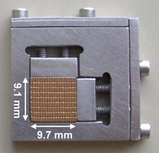
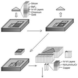
New methods for fabricating semiconductor lasers are being developed by our group. Substrate removal (also known as epitaxial lift-off) techniques have been developed that allow packaging of epitaxially-grown laser materials between two high thermal conductivity copper heat sinks. Such packaging can dramatically improve active region heat dissipation. We are presently applying these new methods to fabrication of improved mid-infrared lasers based on IV-VI semiconductor materials (see Semiconductor Materials). Theoretical analysis of active region heat dissipation has shown that this new way of packaging IV-VI semiconductor mid-IR laser materials will remove the need for liquid nitrogen cooling and enable continuous wave laser operation with thermoelectric cooling modules [1]. Progress in developing substrate removal, metallic bonding of epitaxial layers to copper, and formation of cleaved cavities using the copper bar cleaving tool and procedure outlined in the figures at right are documented in refs. [2-5] listed below. Ability to obtain (110)-oriented cleaved facets of IV-VI semiconductor epitaxial layer material (see electron microscope picture at right) allows use of (111)-oriented MQW structures [6-8] as the active mid-IR laser material. The basic laser fabrication procedure outlined here (see also this Macromedia Flash Movie), can be applied to other laser technologies, such as blue and UV lasers made from GaN and related materials, where the substrate can be removed from the epitaxially-grown laser materials. Benefits in addition to higher operating temperatures include improved reliability, since the laser active region remains cooler, and lower cost production, since an etching step is not needed to make electrical contact to the underlying layers when an insulating substrate such as sapphire is used.
Click
on the pictures for better quality pdf files
References:
[1] K. R. Lewelling and P. J. McCann, “Finite Element Modeling Predicts Possibility of Thermoelectrically-Cooled Lead-Salt Diode Lasers”, IEEE Photonics Technology Letters 9, 297 (1997). (pdf 48K)
[2] H. Z. Wu, X. M. Fang, R. Salas, D. McAlister, and P. J. McCann, “Transfer of PbSe/PbEuSe Epilayers Grown by MBE on BaF2-Coated Si(111)”, Thin Solid Films 352, 277 (1999).

